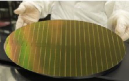
Recently, Wuhan Taiziwei Optoelectronics Technology Co., Ltd. in China launched its T150 A photoresist product, which has successfully passed mass pro...
The process node is not a real resolution, just a marketing term, feature sizes for 5 nm are in the few tens of nanometers. And chinese foundry SMIC uses quadruple patterning to get those feature sizes from less powerful lithography tools.
The photoresist is a component of photolithography, but doesn’t determine the process node on its own. The 120nm quoted here is quite advanced compared to the capitalist products I have found advertised (200nm or so).
Photolithography (also known as optical lithography) is a process used in the manufacturing of integrated circuits. It involves using light to transfer a pattern onto a substrate, typically a silicon wafer.
The process begins with a photosensitive material, called a photoresist, being applied to the substrate. A photomask that contains the desired pattern is then placed over the photoresist. Light is shone through the photomask, exposing the photoresist in certain areas. The exposed areas undergo a chemical change, making them either soluble or insoluble in a developer solution. After development, the pattern is transferred onto the substrate through etching, chemical vapor deposition, or ion implantation processes.


This sounds like a very large feature size given the existence of 3-5 nm process nodes. Or am I missing something here?
The process node is not a real resolution, just a marketing term, feature sizes for 5 nm are in the few tens of nanometers. And chinese foundry SMIC uses quadruple patterning to get those feature sizes from less powerful lithography tools.
The photoresist is a component of photolithography, but doesn’t determine the process node on its own. The 120nm quoted here is quite advanced compared to the capitalist products I have found advertised (200nm or so).
https://en.m.wikipedia.org/wiki/Photolithography