
- cross-posted to:
- technology@lemmy.ml
- technology
- cross-posted to:
- technology@lemmy.ml
- technology
You must log in or # to comment.
When I see these pro-China pieces, I remember that Chinese citizens can’t speak freely, exercise political will, or breathe clean air. As well as China’s actions towards the annexation/militarization of surrounding waters, erasure of Tibetan and Uyghuar cultures, and propagation of destabilizing online propaganda.
This is the best summary I could come up with:
The company has no plans to increase the number of layers with the two Xtacking 4.0 devices currently in development, but the family may get broader over time.
So technically, it will produce 3D NAND arrays with 64 and 116 active layers, which enables wafer fab equipment makers to keep supplying it with necessary tools without directly breaking U.S. export rules (so long as they obtain an export license from the U.S. Department of Commerce).
Plausible advances would include increasing the number of planes to boost parallelism and bitline/wordline optimizations to improve latency.
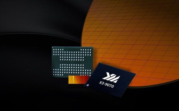
YMTC has been producing its 232-layer 3D TLC NAND memory featuring its Xtacking 3.0 architecture in high volumes for over a year now and more recently expanded its Xtacking 3.0 family with 128-layer 3D TLC and 232-layer 3D QLC offerings that are cheaper, easier to make and which comply with restrictions set by the U.S. government for China.
The company’s Xtacking 3.0 family of products uses string stacking coupled with hybrid bonding that employs an older process node for the CMOS portion of the chip (similar to CuA, but with a separate die).
Therefore, makers of equipment could be using this as yet another loophole to supply wafer fab tools to Chinese entities.
The original article contains 447 words, the summary contains 202 words. Saved 55%. I’m a bot and I’m open source!